
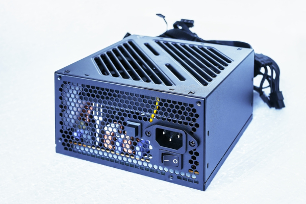
AC/DC power supplies are used in many applications, including consumer electronics, robotics, military, and medical. They can also be referred to by the name AC/DC converter.
An accurate power supply circuit design must start with the PCB due to the current trend of ever-lower power supply voltages, compact footprints, low weight, and high efficiency.
Modern electronic devices often need five or more power rails with unique electrical properties and capabilities. This makes it harder to design the power supply – the part of the electronic device which is essential to its performance, reliability, and longevity.
This article will explore the significant issues engineers have to deal with when designing a PCB for an AC/DC power source, such as output voltage stability and thermal control. It will also examine electromagnetic interference, power lines, and signal integrity. By following the simple rules in this article, the designer can anticipate these issues and prevent them from affecting the PCB design.
AC/DC Power Supplies: Classification
The AC/DC power supply market is vast but can be classified based on critical factors.
- Custom or integrated: Design based only on discrete components or on integrated regulators/converters (IC)
- Technology: switching or linear?
- Electrical characteristics: input voltage range (fixed or variable), output voltage type, output power, efficiency, and more
- Mechanical characteristics: size, weight, type of cooling system, open frame, or enclosed.
About the first point, we can state that, in many cases, the best solution would be to use integrated devices. These offer a variety of advantages, including the simplification of a project, the reduction of BOM, the time to market, and the availability of integrated diagnostics and protection capabilities. For some applications such as high-power, radio frequency, or niche, it may be necessary to use discrete power devices.
The choice of linear or switching power supply, also known as SMPS (short for Switched-Mode Power Supply), depends on the application.
Linear is the oldest but still relevant conversion technology. Although linear AC/DC supplies are not without their advantages, such as low efficiency and power losses, this thrill is used successfully in applications that require high reliability, soft sound, quick recovery, rapid reaction times, and minimal radiated emissions.
LDO (Low DropOut) regulators are an important class of linear power supply. To maximize the efficiency of LDOs, you must minimize the difference between the input voltage (or voltage) and the output voltage. It is also essential to choose regulators that have a low thermal resistance. This will prevent the regulator from rapidly overheating above its optimal operating temperature.
Switching power supplies have become the reference standard for converting AC and DC voltage. This type of conversion operates in a closed loop and is typically non-linear. It uses feedback signals to maintain regulation. Switching regulators may be more efficient and provide better code. However, they can be complicated to design since multiple devices are involved, including significant passive elements like inductors and capacitors.
SMPS power supply units are more complex to design, but they guarantee very high-efficiency levels, surpassing those of the best linear power sources. It allows for better thermal control. The presence of components that switch at high frequencies produces significant amounts of electromagnetic noise. This EMI can affect the quality of the electrical signal to the point that it may cause malfunctions or damage to specific components. This is why linear technology is preferred for electromedical and laboratory instruments.
Layout and Routing
The layout of AC/DC PCBs is crucial since it directly impacts electromagnetic interference (EMI), signal and power integrity, and well and supply efficiency.
A good layout also increases the power conversion efficiency and draws heat away from the hot components. It can also reduce the noise level. In this context, the size of the conductive trace is crucial. It reduces the heat generated by the PCB and increases its reliability under load conditions. A bad layout can lead to problems with high currents or significant voltage differences.
Here are some simple but valid routing rules:
- Use traces as straight and short as possible to connect power devices.
- Avoid inserting sharp edges or curves inside traces, as they can concentrate the electrical field at specific points on the PCB.
- Traces with high voltage differentials must be separated.
- Avoid placing high-voltage traces on the innermost layer of the PCB. In the innermost layer, it’s best to increase the space between the atoms.
- Avoid placing traces with sensitive signals or high data rates near power lines and regulators. This is especially true if the trails are switching types.
- In multilayer PCBs, the traces containing sensitive signals should be separated from the power lines by a ground layer (possibly a solid one).
- Signal traces must never be parallel to the power traces. Power traces are on a separate layer. To reduce noise coupling, signal traces should cross power supply traces with a 90deg angled angle.
- If this is not possible, use Vias to connect multiple layers. You can use Vias to connect various layers if this isn’t possible. Multiple vias may be required for higher currents. It is important to note that vias with a diameter of 14 mils can handle winds as high as 2A. Vias larger than 40 mils can handle currents over 5A.
Use large polygons or solid areas for ground planes. These areas have low impedance paths capable of dispersing sound and handling high return currents. They also allow heat to be dissipated away from critical components. Placing a ground plan on either side can absorb radiated electromagnetic interference (EMI), reduce ground loop noise, and eliminate errors.
AC/DC converters must comply with strict safety and electromagnetic interference regulations. It may be necessary to install EMI filters that meet the standard requirements.
Here are some possible actions:
- Test the EMI effects by performing a preliminary test without any additional filters.
- Find the frequencies that cause the most problems
- Keep power lines and sensitive signals as far as possible from the trace.
- Eliminate ground loops
- You can design an external filter that adds inductive elements to the AC input as a last resort.
The PCB stack up, determined by the arrangement and configuration of the layers within the PCB board, is an essential factor in the board’s performance concerning EMC. A well-designed stack allows for both the reduction of radiations generated by the cables and closed paths (differential modes emissions).
If space allows, it’s always good to include at least one solid plane in the PCB stack-up to provide sufficient electromagnetic shielding and increase immunity to crosstalk and noise. If you have space constraints, you can limit yourself to an area covering all PCB power supply components.