
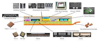
In the late 18th century, the development of computing technology led to a shift in computer architecture, from the 2D drawing era in the 1960s to the machine learning era today, which relies on algorithms, pattern recognition, etc. Computing architectures define how data is processed and transmitted and how the hardware components are connected. Developing new architectures has accelerated the data transfer rate, allowing for better processing.
Designers must overcome several obstacles, including broadband connectivity, low power consumption, system capacity, and others, when designing the next-generation architecture of computers. Other needs include improving system performance metrics and addressing Moore’s Law-related power integrity issues. Diverse materials are used in heterogeneous integration technologies between silicon and packaging processes. This is possible by using inorganic materials and maintaining strict cleanliness standards when integrating chips into wafer fabrication areas.
Applications and Performance of QMC Structure
As can be seen in Figure 1, QMC is a hybrid bonding model that replaces solder to connect chips.
To achieve fab compatibility, an inorganic filler like silicon dioxide replaced the traditional organic filling. This architecture is beneficial for improving the thermomechanical stability of the structure, as it allows flexible chipset arrangements.
QMC can significantly improve performance in multiple computing architectures by adjusting various parameters. These include flexible interconnect options between chipsets for chip-to-chip or chip-to-package connections and high interconnect densities that can be scalable through hybrid bonding. To avoid routing bottlenecks, it is essential to scale both the vertical and lateral interconnect density. This can be seen in Figure 2.
QMC architecture allows this routing, as active chipsets with high-density metallic layers make lateral connections possible. Parallel to this, the Universal Chiplet Interconnect Express standard (UCIE), a modular QMC interface enabling chipset interoperability, was developing a modular QMC interface. This interconnect was ten times more efficient than conventional die-to-die interconnects. As the channels were shorter, chiplets with smaller areas could be used with drivers of smaller sizes with reduced ESD requirements.
Scaled Die-to-Wafer Hybrid Bonding
QMC architecture’s primary goal is to achieve near-monolithic interconnection, which requires a hybrid bonding layer with a much finer pitch. As shown in Figure 3, this bonding layer allows for an improvement of up to nine-fold in interconnect density. The hybrid bonding layer can be defined as damascene layers with particular planarization specs for bonding.
It was necessary to consider several factors to achieve such a high bonding density. To ensure the assembly would produce the desired results, designers had to allow a fine pitch over the metal layer. This assembly can support chipsets that are fully testable and power planes that are independent. It was necessary to make a few changes in the metal stack to achieve this, such as allowing for smaller sizes and overlays.
QMC Process Flow Modules and Enabling Modules
Process Flow
Figure 4 illustrates the basic QMC model. The carrier is attached to the first layer of chipsets, and the ultra-thick fill of oxide is then deposited.
After the chipsets have been created, a permanent bond is made with a top. This top is then bonded to the uppermost layer to provide structural stability. It is important to note that no fab incompatible materials are present during all processing steps.
Deposition of Ultra-Thick Oxide
The thickness of the chipsets must be thicker than the standard thicknesses. They must support the entire chipset height, including the silicon substrate and the metal interconnect.
In QMC, silicon oxide is used for fab compatibility instead of the organic molds commonly used in packaging. The designers faced the challenge of induced stress in the oxide layers since they only form at higher temperatures.